EPD Update Procedure
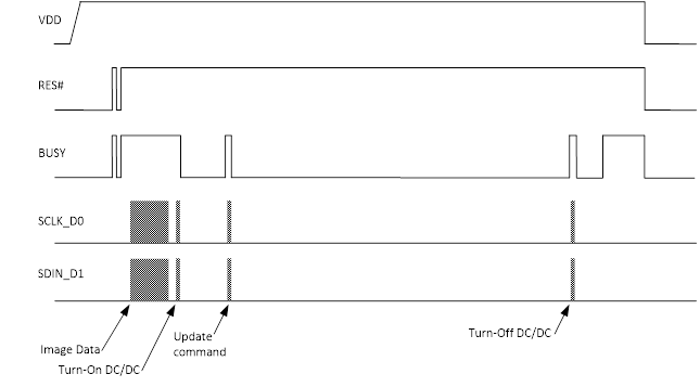
The update procedure includes 8 steps as shown on the right side.
- Power on screen
- Reset the CoG driver
- Read the OTP data
- Initialize the COG driver
- Send the image
- Update the COG
- Stop DC/DC
- Power off screen
Power on screen
The initial state before start has VCC/VDD, /RESET, D/C, /CS, SDA, SCL kept at 0V.
In order to the inrush current will cause other issue. It is recommended to add start DC/DC when VCC/VDD is turned on.
Perform in the following order.
| Step | Pin/Register | Data/Value | Name/Unit | Comment |
|---|---|---|---|---|
| GPIO | POWER | HIGH | External MOSFET power driver | |
| GPIO | D/C | HIGH | Data if HIGH, command if LOW | |
| GPIO | /RESET | HIGH | Panel reset, active LOW | |
| GPIO | Panel /CS | HIGH | SPI chip select, active LOW | |
| GPIO | !BUSY | INPUT | Input, floating | |
| SPI | CLK | SPI clock | ||
| SPI | SDA | SPI data |
Reset the CoG driver
Note
Included in function COG_reset()
| Step | Pin/Register | Data/Value | Name/Unit | Comment |
|---|---|---|---|---|
| GPIO | RESET | LOW | Set RESET HIGH | |
| Delay | 20 10 for 1.54", 2.13" |
ms | Make sure POWER is stable | |
| GPIO | RESET | HIGH | Set RESET HIGH | |
| Delay | 10 10 for 1.54", 2.13" |
ms | ||
| GPIO | RESET | LOW | Set RESET LOW | |
| Delay | 20 20 for 1.54", 2.13" |
ms | ||
| GPIO | RESET | HIGH | Set RESET HIGH | |
| Delay | 10 40 for 1.54", 2.13" |
ms | ||
| GPIO | BUSY | HIGH? | Proceed to next step when HIGH Otherwise, continue waiting |
|
| Delay | 10 10 for 1.54", 2.13" |
ms |
Proceed to next step “Read the OTP data”.
If the OTP data is already read and available, proceed to Initialise the COG driver.
Read the OTP data
Note
Included in function COG_getDataOTP()
This step is performed once, as long as the host retains the values. If the host loses the values, the host should perform this step again.
Info
The maximum clock speed of the display is 2.5MHz (Read).
The SPI sequence for reading the OTP follows:
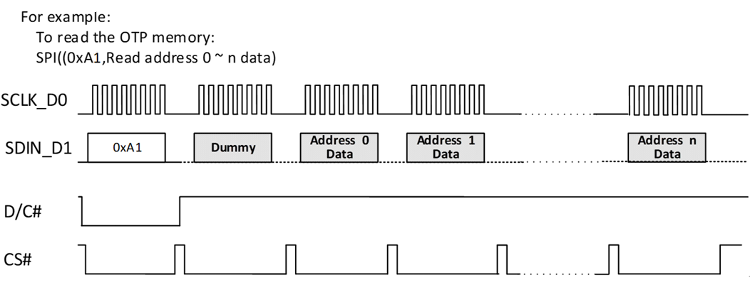
There are two bank spaces in the OTP memory. When the data are read out, the first step is to determine which space is the active space (Bank0 or Bank1).
If the address 0 data is “0xa5”, the active space is Bank0; otherwise, the active space is Bank1.
| EPD Size | Active bank | OTP range |
|---|---|---|
| 1.54", 2.13", 2.66", 2.9" | bank0 | 0x1500-152F |
| 1.52", 2.06” | bank0 | 0xD80-0xDAF |
| 4.2", 4.37" | bank0 | 0x1500-156F |
| bank1 | 0x1570-15DF |
| Step | Pin/Register | Data/Value | Name/Unit | Comment |
|---|---|---|---|---|
| GPIO | /CS | LOW | Select | |
| GPIO | D/C | LOW | Command mode | |
| SPI3 | 0x70 | SPI3 = SCK, SDIO, CS plus D/C | ||
| GPIO | D/C | HIGH | Data mode | |
| SPI3 | Read 2 bytes | Read the chip ID 0x03, 0x02 for 1.54", 2.13, (2.66" old model) 0x83, 0x02 for 2.66" 0x85, 0x02 for 2.9" 0x06, 0x05 for 4.2" 0x0B, 0x04 for 4.37" |
||
| SPI3 | 0xa4 | [0x15, 0x00, 0x01] | Sets the start address for OTP reading | |
| GPIO | BUSY | HIGH? | Proceed to next step when HIGH Otherwise, continue waiting |
|
| SPI3 | 0xa1 | Assigns the start address for OTP reading | ||
| SPI3 | 1 byte | Reads 1 dummy byte | ||
| SPI3 | 48 bytes for 1.54", 2.13", 2.66", 2.9" 112 bytes for 4.2", 4.37" |
Reads OTP data bytes | ||
| GPIO | RESET | LOW | Set RESET LOW | |
| Delay | 40 | ms | ||
| GPIO | RESET | HIGH | Set RESET HIGH | |
| Delay | 10 | ms | ||
| GPIO | BUSY | HIGH? | Proceed to next step when HIGH Otherwise, continue waiting |
|
| GPIO | /CS | HIGH | Unselect |
Then, follow the COG reset procedure in the previous section.
1.52”, 2.06”
| Step | Pin/Register | Data/Value | Name/Unit | Comment |
|---|---|---|---|---|
| GPIO | /CS | LOW | Select | |
| GPIO | D/C | LOW | Command mode | |
| SPI3 | 0x70 | SPI3 = SCK, SDIO, CS plus D/C | ||
| GPIO | D/C | HIGH | Data mode | |
| SPI3 | Read 2 bytes | Read the chip ID 0x48, 0x01 for 1.52" 0xC9, 0x01 for 2.06" |
||
| SPI3 | 0xF0 | 0x0B | ||
| SPI3 | 0x90 | |||
| GPIO | BUSY | HIGH? | Proceed to next step when HIGH Otherwise, continue waiting |
|
| SPI3 | 0xA2 | 0x33 | ||
| SPI3 | 0xA0 | |||
| GPIO | BUSY | HIGH? | Proceed to next step when HIGH Otherwise, continue waiting |
|
| SPI3 | 0xF6 | [0x2D, 0x80] for 1.52" [0x0D, 0x80] for 2.06" |
||
| SPI3 | 0x92 | Assigns the start address for OTP reading | ||
| SPI3 | 1 byte | Reads 1 dummy byte | ||
| SPI3 | 48 bytes | Reads OTP data bytes | ||
| GPIO | RESET | LOW | Set RESET LOW | |
| Delay | 40 | ms | ||
| GPIO | RESET | HIGH | Set RESET HIGH | |
| Delay | 10 | ms | ||
| GPIO | BUSY | HIGH? | Proceed to next step when HIGH Otherwise, continue waiting |
|
| GPIO | /CS | HIGH | Unselect |
Then, follow the COG reset procedure in the previous section.
Store the OTP data in memory to avoid reading it at each update.
Initialize the COG Driver
Note
Included in function COG_initial()
1.54”, 2.13”, 2.66”
Note
The ambient temperature value comes from your chosen external temperature sensor. Default value in our demo is 25C. Update this when working outside room temperature range.
| Step | Pin/Register | Data/Value | Name/Unit | Comment |
|---|---|---|---|---|
| SPI | 0xe0 | 0x02 | 1 byte | |
| SPI | 0xe6 | Temperature | 1 byte | |
| SPI | 0xa5 | 0 byte | ||
| GPIO | BUSY | HIGH? | Proceed to next step when HIGH Otherwise, continue waiting |
|
| SPI | 0x01 | OTP[16] | 1 byte | |
| SPI | 0x00 | OTP[17-18] | 2 bytes | |
| SPI | 0x03 | OTP[30-32] | 3 bytes | |
| SPI | 0x06 | OTP[23-29] | 7 bytes | |
| SPI | 0x50 | OTP[39] | 1 byte | |
| SPI | 0x60 | OTP[40-41] | 2 bytes | |
| SPI | 0x61 | OTP[19-22] | 4 bytes | |
| SPI | 0xe7 | OTP[33] | 1 byte | |
| SPI | 0xe3 | OTP[42] | 1 byte | |
| SPI | 0x4d | OTP[43] | 1 byte | |
| SPI | 0xb4 | OTP[44] | 1 byte | |
| SPI | 0xb5 | OTP[45] | 1 byte | |
| SPI | 0xe9 | 0x01 | 1 byte | |
| SPI | 0x30 | 0x08 | 1 byte |
1.52”, 2.06”
Note
The ambient temperature value comes from your chosen external temperature sensor. Default value in our demo is 25C. Update this when working outside room temperature range.
| Step | Pin/Register | Data/Value | Name/Unit | Comment |
|---|---|---|---|---|
| SPI | 0xe0 | 0x02 | 1 byte | |
| SPI | 0xe6 | Temperature | 1 byte | |
| SPI | 0xa5 | 0 byte | ||
| GPIO | BUSY | HIGH? | Proceed to next step when HIGH Otherwise, continue waiting |
|
| SPI | 0x01 | OTP[16-17] | 2 bytes | |
| SPI | 0x00 | OTP[18-19] | 2 bytes | |
| GPIO | BUSY | HIGH? | Proceed to next step when HIGH Otherwise, continue waiting |
|
| SPI | 0x61 | OTP[20-23] | 4 bytes | |
| GPIO | BUSY | HIGH? | Proceed to next step when HIGH Otherwise, continue waiting |
|
| SPI | 0x06 | OTP[24-27] | 7 bytes | |
| SPI | 0x03 | OTP[30] | 1 byte | |
| SPI | 0xe7 | OTP[33] | 1 byte | |
| SPI | 0x65 | OTP[34-37] | 4 bytes | |
| SPI | 0x30 | OTP[38] | 1 byte | |
| SPI | 0x50 | OTP[39] | 1 byte | |
| SPI | 0x60 | OTP[40-41] | 2 bytes | |
| SPI | 0xe3 | OTP[42] | 1 byte | |
| SPI | 0x62 | OTP[43-44] | 2 bytes | |
| SPI | 0xe9 | 0x01 | 1 byte |
2.9Ӧ
Note
The ambient temperature value comes from your chosen external temperature sensor. Default value in our demo is 25C. Update this when working outside room temperature range.
| Step | Pin/Register | Data/Value | Name/Unit | Comment |
|---|---|---|---|---|
| SPI | 0xe0 | 0x02 | 1 byte | |
| SPI | 0xe6 | Temperature | 1 byte | |
| SPI | 0xa5 | 0 byte | ||
| GPIO | BUSY | HIGH? | Proceed to next step when HIGH Otherwise, continue waiting |
|
| SPI | 0x01 | OTP[16] | 1 byte | |
| SPI | 0x00 | OTP[17-18] | 2 bytes | |
| SPI | 0x61 | OTP[19-22] | 4 bytes | |
| SPI | 0x06 | OTP[23-29] | 7 bytes | |
| SPI | 0x03 | OTP[30-32] | 3 bytes | |
| SPI | 0xe7 | OTP[33] | 1 byte | |
| SPI | 0x65 | OTP[34-37] | 4 bytes | |
| SPI | 0x30 | OTP[38] | 1 byte | |
| SPI | 0x50 | OTP[39] | 1 byte | |
| SPI | 0x60 | OTP[40-41] | 2 bytes | |
| SPI | 0xe3 | OTP[42] | 1 byte | |
| SPI | 0x4d | OTP[43] | 1 byte | |
| SPI | 0xb4 | OTP[44] | 1 byte | |
| SPI | 0xb5 | OTP[45] | 1 byte | |
| SPI | 0xb6 | OTP[46] | 1 byte | |
| SPI | 0xbe | OTP[47] | 1 byte | |
| SPI | 0xe9 | 0x01 | 1 byte |
4.2Ӧ
Note
The ambient temperature value comes from your chosen external temperature sensor. Default value in our demo is 25C. Update this when working outside room temperature range.
| Step | Pin/Register | Data/Value | Name/Unit | Comment |
|---|---|---|---|---|
| SPI | 0xe0 | 0x02 | 1 byte | |
| SPI | 0xe6 | Temperature | 1 byte | |
| SPI | 0x01 | OTP[16] | 1 byte | |
| SPI | 0x00 | OTP[17-18] | 2 bytes | |
| SPI | 0x03 | OTP[30-32] | 3 bytes | |
| SPI | 0x06 | OTP[23-25] | 3 bytes | |
| SPI | 0x50 | OTP[39] | 1 byte | |
| SPI | 0x60 | OTP[40-41] | 2 bytes | |
| SPI | 0x61 | OTP[19-22] | 4 bytes | |
| SPI | 0xe3 | OTP[42] | 1 byte | |
| SPI | 0xe7 | OTP[33] | 1 byte | |
| SPI | 0x65 | OTP[34-37] | 4 bytes | |
| SPI | 0x30 | OTP[38] | 1 byte | |
| SPI | 0xe9 | 0x01 | 1 byte | |
| SPI | 0x04 | 0 byte |
4.37Ӧ
Note
The ambient temperature value comes from your chosen external temperature sensor. Default value in our demo is 25C. Update this when working outside room temperature range.
| Step | Pin/Register | Data/Value | Name/Unit | Comment |
|---|---|---|---|---|
| SPI | 0xe6 | Temperature | 1 byte | |
| SPI | 0xe0 | 0x02 | 1 byte | |
| SPI | 0xa5 | 0 byte | ||
| GPIO | BUSY | HIGH? | Proceed to next step when HIGH Otherwise, continue waiting |
|
| SPI | 0x00 | OTP[17-18] | 2 bytes | |
| SPI | 0x01 | OTP[16] | 1 byte | |
| SPI | 0x03 | OTP[30-32] | 3 bytes | |
| SPI | 0x06 | OTP[23-25] | 3 bytes | |
| SPI | 0x30 | OTP[38] | 1 byte | |
| SPI | 0x50 | OTP[39] | 1 byte | |
| SPI | 0x60 | OTP[40-41] | 2 bytes | |
| SPI | 0x61 | OTP[19-22] | 4 bytes | |
| SPI | 0x65 | OTP[34-37] | 4 bytes | |
| SPI | 0xe7 | OTP[33] | 1 byte | |
| SPI | 0xe3 | OTP[42] | 1 byte | |
| SPI | 0xe9 | 0x01 | 1 byte |
Send the Image
Note
Included in function COG_sendImageDataNormal()
| Step | Pin/Register | Data/Value | Name/Unit | Comment |
|---|---|---|---|---|
| SPI | 0x10 | Image data | The data is the NEW image data that you want displayed next moment |
The index of the image buffer is 0x10.
Sending the image data array to this register requires defining the size of the array. To do so, take note of the buffer size according to your EPD screen size, as seen below.
| Size | 1.52” | 1.54” | 2.06” | 2.13” | 2.66” | 2.9” | 4.2” | 4.37” |
|---|---|---|---|---|---|---|---|---|
| Bytes | 10000 | 5776 | 7936 | 5512 | 11248 | 16128 | 30000 | 21120 |
There are 2-bit data per pixel to define 4 colors.
| Data | Colour |
|---|---|
| 00 | Black |
| 01 | White |
| 10 | Yellow |
| 11 | Red |
Example
The first byte represents the 1st…4th pixels of the first line.
The second byte represents the 5th…8th pixels of the first line, and so on.

Update the COG
Note
Included in function COG_update()
Send the Update Command
For 1.52”, 1.54”, 2.06”, 2.13”, 2.66”, 2.9”
| Step | Pin/Register | Data/Value | Name/Unit | Comment |
|---|---|---|---|---|
| SPI | 0x04 | Power on DC/DC | ||
| GPIO | !BUSY | HIGH? | Wait for !BUSY = HIGH | |
| SPI | 0x12 | 0x00 | Display refresh | |
| GPIO | !BUSY | HIGH? | Wait for !BUSY = HIGH |
For 4.2Ӧ
| Step | Pin/Register | Data/Value | Name/Unit | Comment |
|---|---|---|---|---|
| SPI | 0x12 | 0x00 | Display refresh | |
| GPIO | !BUSY | HIGH? | Wait for !BUSY = HIGH |
For 4.37Ӧ
| Step | Pin/Register | Data/Value | Name/Unit | Comment |
|---|---|---|---|---|
| SPI | 0xff | 0xa5 | 1 byte | |
| SPI | 0xef | OTP[43-50] | 8 bytes | |
| SPI | 0xc3 | OTP[64] | 1 byte | |
| SPI | 0xdc | OTP[59] | 1 byte | |
| SPI | 0xdd | OTP[60] | 1 byte | |
| SPI | 0xde | OTP[61] | 1 byte | |
| SPI | 0xfd | OTP[65] | 1 byte | |
| SPI | 0xe8 | OTP[62] | 1 byte | |
| SPI | 0xda | OTP[63] | 1 byte | |
| SPI | 0xc9 | OTP[67] | 1 byte | |
| SPI | 0xa8 | OTP[66] | 1 byte | |
| SPI | 0xff | 0xe3 | 1 byte | |
| SPI | 0x04 | 0 byte | ||
| GPIO | BUSY | HIGH? | Proceed to next step when HIGH Otherwise, continue waiting |
|
| SPI | 0xff | 0xa5 | 1 byte | |
| SPI | 0xef | OTP[51-58] | 8 bytes | |
| SPI | 0xc3 | OTP[64] | 1 byte | |
| SPI | 0xdc | OTP[59] | 1 byte | |
| SPI | 0xdd | OTP[60] | 1 byte | |
| SPI | 0xde | OTP[61] | 1 byte | |
| SPI | 0xfd | OTP[65] | 1 byte | |
| SPI | 0xe8 | OTP[62] | 1 byte | |
| SPI | 0xda | OTP[63] | 1 byte | |
| SPI | 0xc9 | OTP[67] | 1 byte | |
| SPI | 0xa8 | OTP[66] | 1 byte | |
| SPI | 0xff | 0xe3 | 1 byte | |
| SPI | 0x12 | 0x00 | 1 byte | |
| GPIO | BUSY | HIGH? | Proceed to next step when HIGH Otherwise, continue waiting |
Stop DC/DC
Note
Included in function COG_stopDCDC()
All sizes
| Step | Pin/Register | Data/Value | Name/Unit | Comment |
|---|---|---|---|---|
| SPI | 0x02 | 0x00 | Turn off DC/DC | |
| GPIO | !BUSY | HIGH? | Wait for !BUSY = HIGH |
For 1.52”, 2.06”
| Step | Pin/Register | Data/Value | Name/Unit | Comment |
|---|---|---|---|---|
| SPI | 0x07 | 0xa5 | 1 byte |
For 4.2Ӧ
| Step | Pin/Register | Data/Value | Name/Unit | Comment |
|---|---|---|---|---|
| SPI | 0x00 | OTP[26-27] | 2 bytes |
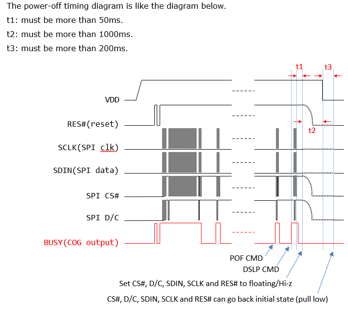
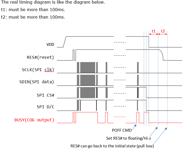
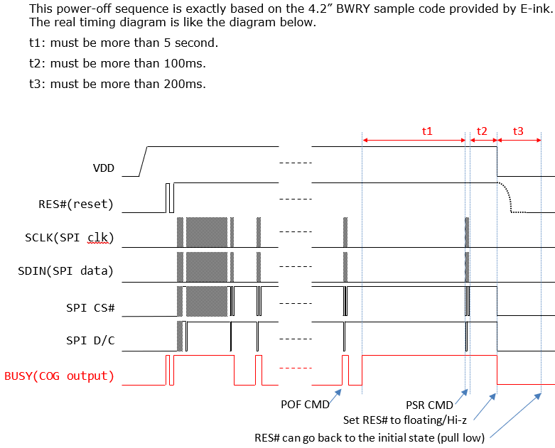
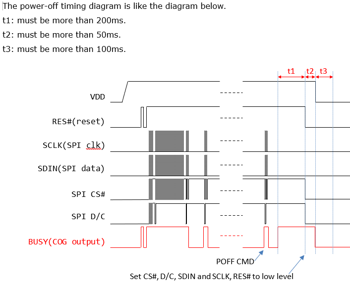
Power the screen off
| Step | Pin/Register | Name/Unit | Name/Unit | Comment |
|---|---|---|---|---|
| GPIO | D/C | LOW | Data if HIGH, command if LOW | |
| GPIO | /RESET | LOW | Panel reset, active low | |
| GPIO | Panel /CS | LOW | SPI chip select, active low | |
| GPIO | !BUSY | Input, floating | ||
| GPIO | POWER | LOW | External MOSFET power driver | |
| SPI | CLK | SPI clock | ||
| SPI | SDA | SPI data |
For 1.52”, 2.06”
For 2.66”, 2.9”
For 4.2Ӧ
For 4.37Ӧ
The EPD update procedure is completed.