Update Procedure
COG Power On
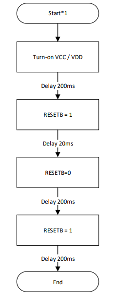
Initial states
- VCC/VDD = 0
- RESETB = 0
- CSB = 0
- SDA = 0
- SCL = 0
Danger
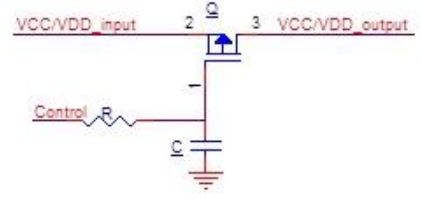
In order to avoid current surge, it is recommended to include a soft-start when VCC/VDD is activated.
Read OTP Data
The 128-bytes section of OTP have saved the user-defined data(OTP address from 0x0EE8 to 0x0F67) that includes the information of the display and soft-start parameters. The section will introduce how to read out the data through the SPI.
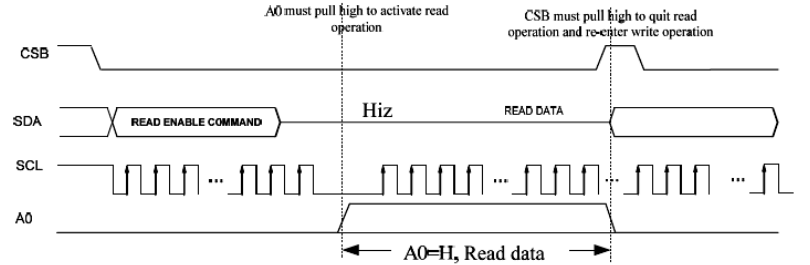
After the READ ENABLE command is set, SDA and A0 must both be set HIGH to activate the READ operation.
When this is done, CSB must be set HIGH once to halt the READ operation.
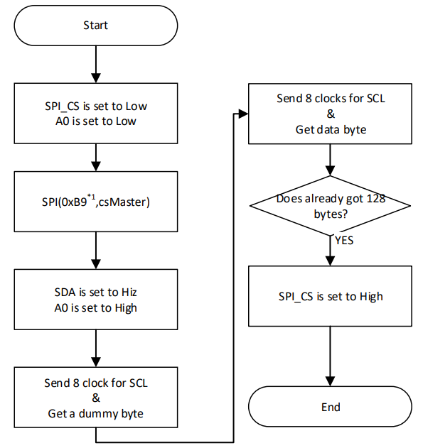
Apply command 0xB9 to read OTP data from the OTP addresses 0x0EE8 to 0x0F67.
COG Initialize
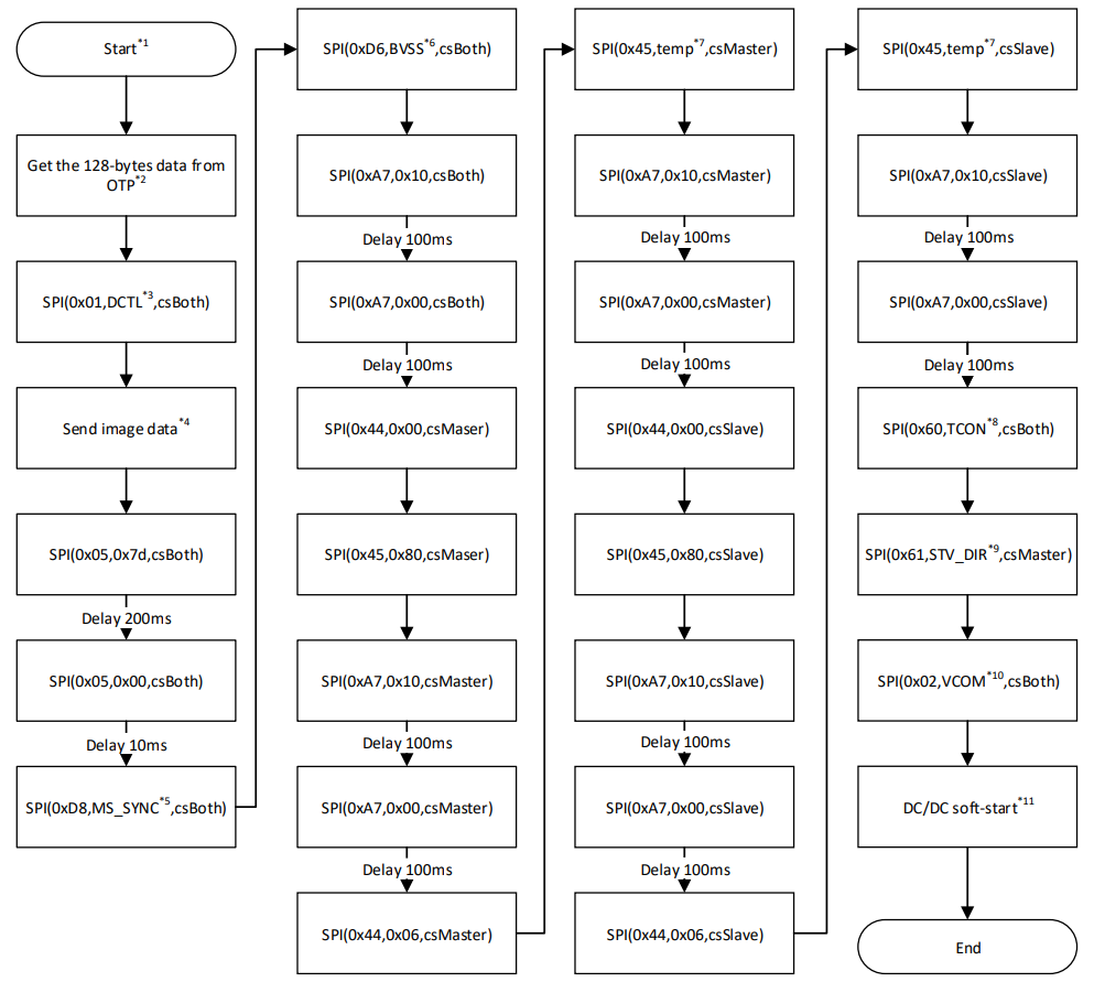
Comments
- Item 2 See Read OTP Data
- Item 4 See Send Image to EPD
- Item 7 See Temperature Setup below
- Item 11 See DC-DC Soft Start
Temperature Setup
The acceptable temperature range is -40 to 87 deg Celsius, with 0.5 deg C per step resolution.
For example:
| Value (deg C) | HEX |
|---|---|
| -40 | 0x00 |
| 0 | 0x50 |
| 25 | 0x82 |
| 87 | 0xFE |
The following data values are read from
| Data | Register Address - OTP Memory | |
|---|---|---|
| DCTL | 0x10 | |
| MS_SYNC | 0x1C | |
| BVSS | 0x1D | |
| TCON | 0x0B | |
| STV_DIR | 0x1B | |
| VCOM | 0x11 |
Send Image to EPD
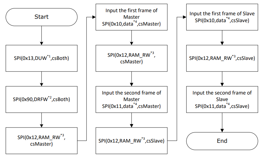
Comments
| Register | Value |
|---|---|
| DUW | 0x15 to 0x1A |
| DRFW | 0x0C to 0x0F |
| RAM_RW | 0x12 to 0x14 |
Info
Item 4: Data size of 40,320 bytes
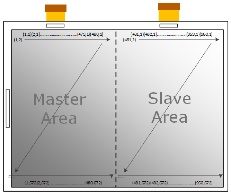
Image Format
The data of image frame, one bit represents 1 pixel. The first byte represents the 1st to 8th pixels of the first line. The second byte, 9th to 16th pixels of the first line. And so on.
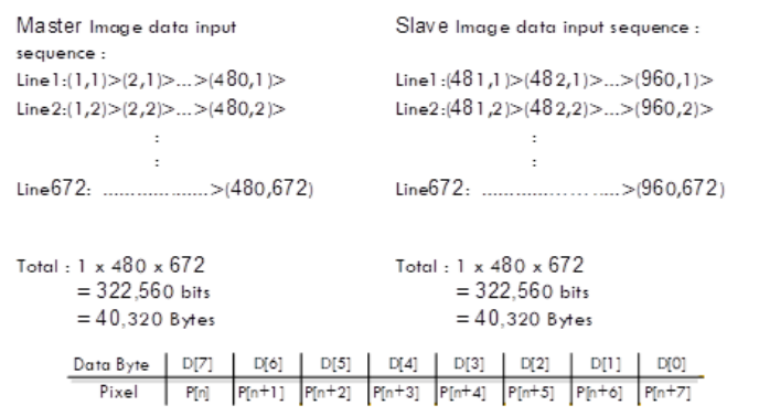
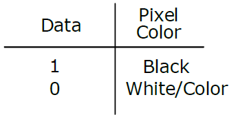
- First Frame
The frame is the “black” frame. The data “1” represents the black color pixel and data “0” represents both white and color pixel.
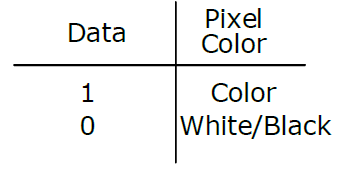
- Second Frame
The frame is the “Color” frame. The data “1” represents the color pixel and data “0” represents both black and white pixel.
DC/DC soft-start
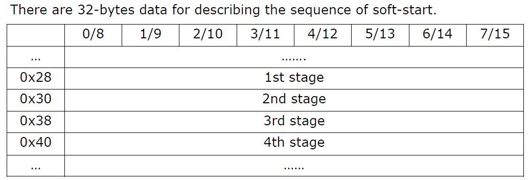
The sequence totally has 4 stages. Each stage has 8-byte parameters. The bytes of each stage can be interpreted in 2 ways.
Data structure and definition
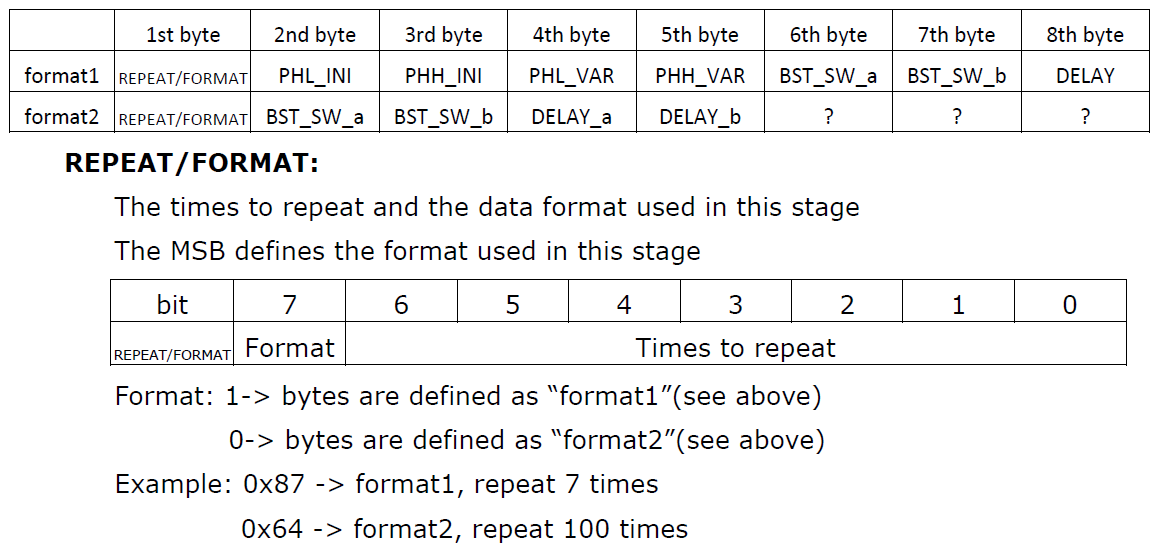
- PHL_INI
Define the initial value of PHL (the first data of the register 0x51)
- PHH_INI
Define the initial value of PHH (the second data of the register 0x51)
- PHL_VAR
The byte represents the changing value of PHL with each iteration (REPEAT)
- PHH_VAR
The byte represents the changing value of PHH with each iteration (REPEAT)
- BST-SW-a
BST_SW setting is the power on/off manager (Reg 0x09) at the start of the phase
- BST-SW-b
BST_SW setting is the power on/off manager (Reg 0x09) at the start of the phase
Both PHL_VAR_n and PHH_VAR_n could be a negative number. The negative number is represented by 2’s complement. Example: -5 equals 0xFB
- DELAY
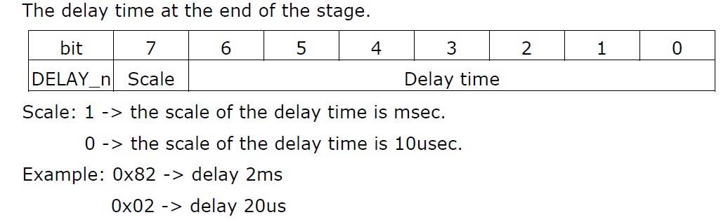
- DELAY_a
Same as “DELAY” but inserted after BST-SW-a
- DELAY_b
Same as “DELAY” but inserted after BST-SW-b
Flowchart
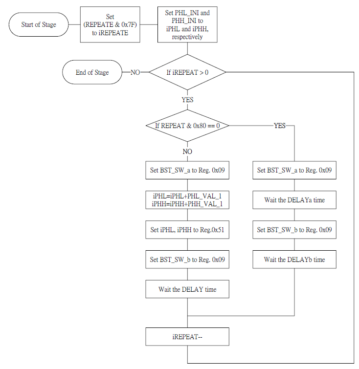
Info
Note: iREPEAT, iPHH, iPHL are variable
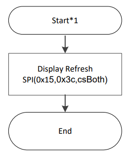
Update Command
Turn off DC/DC
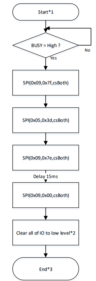
Warning
VCC/VDD, RESETB, A0, M_CSB_, S__CSB, SCK, MOSI should all be LOW before END.