EPD Update Procedure
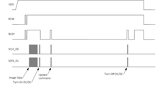
The update procedure includes 8 steps as shown on the right side.
- Power on screen
- Reset the CoG driver
- Read the OTP data
- Initialize the COG driver
- Send the image
- Update the COG
- Stop DC/DC
- Power off screen
Power on screen
The initial state before start has VCC/VDD, /RESET, D/C, /CS, SDA, SCL kept at 0V.
In order to the inrush current will cause other issue. It is recommended to add start DC/DC when VCC/VDD is turned on.
Perform in the following order.
| Step | Pin/Register | Data/Value | Name/Unit | Comment |
|---|---|---|---|---|
| GPIO | POWER | HIGH | External MOSFET power driver | |
| GPIO | D/C | HIGH | Data if HIGH, command if LOW | |
| GPIO | /RESET | HIGH | Panel reset, active LOW | |
| GPIO | Panel /CS | HIGH | SPI chip select, active LOW | |
| GPIO | !BUSY | INPUT | Input, floating | |
| SPI | CLK | SPI clock | ||
| SPI | SDA | SPI data |
Reset the CoG driver
Note
Included in function COG_reset()
| Step | Pin/Register | Data/Value | Name/Unit | Comment |
|---|---|---|---|---|
| GPIO | POWER | HIGH | Set POWER HIGH | |
| Delay | 5 | ms | Make sure POWER is stable | |
| GPIO | RESET | HIGH | Set RESET HIGH | |
| Delay | 5 | ms | ||
| GPIO | RESET | LOW | Set RESET LOW | |
| Delay | 10 | ms | ||
| GPIO | RESET | HIGH | Set RESET HIGH | |
| Delay | 20 | ms | ||
| GPIO | !BUSY | **HIGH? | WHEN LOW IC type error (Wrong application note) DISCONTINUE USE |
|
| WHEN HIGH Continue below |
||||
| SPI | 0x00 | 0x0E | Soft-reset | |
| 0x12 | -- | If using 1.52” |
Warning
The BUSY pin rule is inverted when using 1.52”. Wait for BUSY to turn LOW before proceeding.
Proceed to next step “Read the OTP data”.
If the OTP data is already read and available, proceed to Initialise the COG driver.
Read the OTP data
Note
Included in function COG_getDataOTP()
This step is performed once, as long as the host retains the values. If the host loses the values, the host should perform this step again.
Info
The maximum clock speed of the display is 2.5MHz (Read).
There are two bank spaces in the OTP memory. When the data are read out, the first step is to determine which space is the active space (Bank0 orBank1).
If the address 0 data is “0xa5”, the active space is Bank0; otherwise, the active space is Bank1.
The SPI sequence for reading the OTP follows:
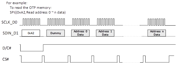
| Step | Pin/Register | Data/Value | Name/Unit | Comment |
|---|---|---|---|---|
| GPIO | /CS | LOW | Select | |
| GPIO | D/C | LOW | Command mode | |
| SPI3 | 0xa2 | SPI3 = SCK, SDIO, CS plus D/C | ||
| GPIO | D/C | HIGH | Data mode | |
| SPI3 | Read 1 byte | Read dummy data | ||
| SPI3 | Read 1 byte | Check active space address. If “0xa5”, active space is Bank0. Else, Bank1. See table below. |
||
| SPI3 | Read 1 byte | Keep reading and discard bytes until the Bank address is reached. | ||
| SPI3 | Read 2 bytes | Read and store the PSR data. | ||
| GPIO | /CS | HIGH | Unselect |
| EPD Size | Active bank | PSR[0] Addr. | PSR[1] Addr. |
|---|---|---|---|
| 1.54", 2.66", 2.7", 3.5", 3.7", 4.37" | bank0 | 0xFB4 | 0xFB5 |
| bank1 | 0x1FB4 | 0x1FB5 | |
| 2.06”, 2.13" | bank0 | 0xB1B | 0xB1C |
| bank1 | 0x171B | 0x171C | |
| 4.2" | bank0 | 0xB1F | 0xB20 |
| bank1 | 0x171F | 0x1720 |
Store the OTP data in memory to avoid reading it at each update.
Proceed to next step Initialise the COG driver.
Initialize the COG Driver
Note
Included in function COG_initial()
Warning
This next sequence will depend on the EPD size being used.
2.9” and 1.52” have their unique sequence for this section.
Danger
Operating outside the acceptable temperature range may damage the panel.
For 2.9” EPD
| Step | Pin/Register | Data/Value | Name/Unit | Comment |
|---|---|---|---|---|
| SPI | 0xe5 | TSSET | Normal update – See note below Input temperature |
|
| TSSET + 0x40 | Fast update – See note below Input temperature |
|||
| SPI | 0xe0 | 0x02 | Active Temperature | |
| SPI | 0x4d | 0x55 | ||
| 0xe9 | 0x02 | |||
| SPI | 0x50 | 0x07 | Fast update only |
For 1.52” EPD
| Step | Pin/Register | Data/Value | Name/Unit | Comment |
|---|---|---|---|---|
| SPI | 0x1a | TSSET | ||
| 0x22 | 0xd7 | Normal update | ||
| SPI | 0x3c | 0xc0 | Fast update | |
| 0x22 | 0xdf |
For other small sizes
1.54”, 2.06”, 2.13”, 2.66”, 2.7”, 3.5”, 3.7”, 4.2” and 4.37”
| Step | Pin/Register | Data/Value | Name/Unit | Comment |
|---|---|---|---|---|
| SPI | 0xe5 | TSSET | Normal update – See note below Input temperature |
|
| TSSET + 0x40 | Fast update – See note below Input temperature |
|||
| SPI | 0xe0 | 0x02 | Active Temperature | |
| SPI | 0x00 | PSR | Normal update Input temperature |
|
| 0x00 | PSR[0] | 0x10 PSR[1] | 0x02 |
Fast update | ||
| SPI | 0x50 | 0x07 |
Calculation of TSSET from tempC temperature in C
Note
TSSET refers to the ambient temperature. This value comes from your chosen external temperature sensor. Default value in our demo is 25C. Update this when working outside room temperature range.
| Normal update | Fast update | |
|---|---|---|
| Definition | TSSET is an index of the normal update. | TSSET is an index of the fast update. |
| Range | The acceptable range of temperature is -15°C to +60°C and 1°C per step. | The acceptable range of temperature is +0°C to +50°C and 1°C per step. |
| Check tempC | -15 <= tempC <= +60 | 0 <= tempC <= +50 |
| Value TSSET | TSSET = tempC | TSSET = tempC |
| Low value check | 0xF1 | 0x00 |
| High value check | 0x3C | 0x32 |
Send the Image
Note
Included in function COG\_sendImageDataNormal() and function COG\_sendImageDataFast()
| Step | Pin/Register | Data/Value | Name/Unit | Comment |
|---|---|---|---|---|
| SPI | 0x50 | 0x27 | Fast Update only | |
| SPI | 0x10 | Image array | DTM1 | New image for Normal Old image for Fast |
| SPI | 0x13 | Image array | DTM2 | 0x00 dummy array for Normal New image for Fast |
| SPI | 0x50 | 0x07 | Fast Update only |
For 1.52Ӧ
| Step | Pin/Register | Data/Value | Name/Unit | Comment |
|---|---|---|---|---|
| SPI | 0x24 | Image array | DTM1 | New image for Normal Old image for Fast |
| SPI | 0x26 | Image array | DTM2 | 0x00 dummy array for Normal New image for Fast |
Content of DTM1 and DTM2
| Normal update | Fast update | |
|---|---|---|
| DTM1 | DTM1: the data is the NEW image data that you want to display next moment. | DTM1: the data is the NEW image data that you want displaying next moment. |
| DTM2 | Normal update – DTM2 image is dummy data. It just needs to be filled with the enough amount of 0x00. | Fast update – DTM2 image is the OLD image data that already displayed on the EPD. |
Note
Image order is important when calling Fast Update, especially when used in succession. Unlike with Normal Update, two images are always used with Fast Update: the old and new images. Note that the new image of the first Fast Update call becomes the old image of the second succeeding Fast Update call.
Neglecting this order will result to ghosting and improper image display.
| EPD Size | Size n (bytes) |
|---|---|
| 1.52 | 5000 |
| 1.54 | 2888 |
| 2.06 | 3968 |
| 2.13 | 2756 |
| 2.66 | 5624 |
| 2.7 | 5808 |
| 2.9 | 8064 |
| 3.5 | 13920 |
| 3.7 | 12480 |
| 4.2 | 15000 |
| 4.37 | 10560 |
The EPD needs to receive both first and second frame data each updating.
The index of the first frame is 0x10 and the second frame is 0x11.
The data of image frame, one bit represents 1 pixel.

Example
The first byte represents the 1st…8th pixels of the first line.
The second byte represents the 9th…16th pixels of the first line, and so on.
Data 1 represents a black colour pixel and data 0 represents a white colour pixel.
Update the COG
Note
Included in function COG_update()
Send the Update Command
| Step | Pin/Register | Data/Value | Name/Unit | Comment |
|---|---|---|---|---|
| SPI | 0x04 | - | Start DC/DC | |
| GPIO | !BUSY | HIGH? | Wait for !BUSY = HIGH | |
| SPI | 0x12 | - | Refresh display | |
| GPIO | !BUSY | HIGH? | Wait for !BUSY = HIGH |
For 1.52Ӧ
| Step | Pin/Register | Data/Value | Name/Unit | Comment |
|---|---|---|---|---|
| GPIO | BUSY | LOW? | Wait for BUSY = LOW | |
| SPI | 0x20 | - | Refresh display | |
| GPIO | BUSY | LOW? | Wait for BUSY = LOW |
Stop DC/DC
Note
Included in function COG_stopDCDC()
| Step | Pin/Register | Data/Value | Name/Unit | Comment |
|---|---|---|---|---|
| GPIO | !BUSY | HIGH? | Wait for !BUSY = HIGH | |
| SPI | 0x02 | - | Stop DC/DC |
Warning
Skip this section when using 1.52”
Power the screen off
| Step | Pin/Register | Name/Unit | Name/Unit | Comment |
|---|---|---|---|---|
| GPIO | D/C | LOW | Data if HIGH, command if LOW | |
| GPIO | /RESET | LOW | Panel reset, active low | |
| GPIO | Panel /CS | LOW | SPI chip select, active low | |
| GPIO | !BUSY | Input, floating | ||
| GPIO | POWER | LOW | External MOSFET power driver | |
| SPI | CLK | SPI clock | ||
| SPI | SDA | SPI data |
Warning
Skip !BUSY when using 1.52”
The EPD update procedure is completed.