Update Procedure
Read OTP Memory
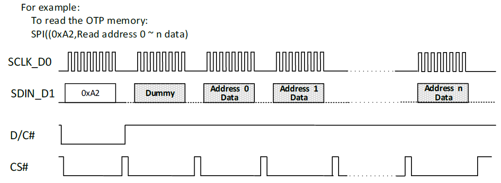
Read OTP memory to get PSR data, PSR data must be sent in the next chapter. The OTP memory can be read by register index 0xA1, the first reading data may be dummy.
There are two sectors of memory in OTP that were programmed as the User-defined data and COG initial data.
| Address | Data | Description |
|---|---|---|
| 0x0000 - 0x14FF | Eink Reserves | |
| 0x1500 | Check Code | Checks whether OTP data is valid. Value should be `0xa5` |
| 0x1501 | Layout Rev | A unique version-number which identifies the memory layout |
| 0x1502 | COG Type | COG ID |
| 0x1503 | Vendor | Vendor ID |
| 0x1504 | Waveform Rev | Revision number of the waveform |
| 0x1505 - 0x150A | FPL Lot Name | The 6-byte means the FPL lot name, it is 6-character ASCII encoding. For example, FPL-lot "SMM069" will be written as 0x53,0x4D,0x4D,0x30,0x36,0x39 |
| 0x150B | Color | The colors supported by this EPD 0x04 -> It supports black/white/red/yellow |
| 0x150C - 0x150F | Eink Reserves | |
| 0x1510 - 0x152F | COG Initial Data | The data of this sector are the necessary IC initial data. These data need to be read out for IC initialization. |
| 0x1530 - ... | Eink Reserves |
COG Power On
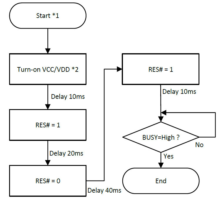
Initial state the VCC/VDD, RES#, CS#, SDIN, SCLK, BS, D/C = 0
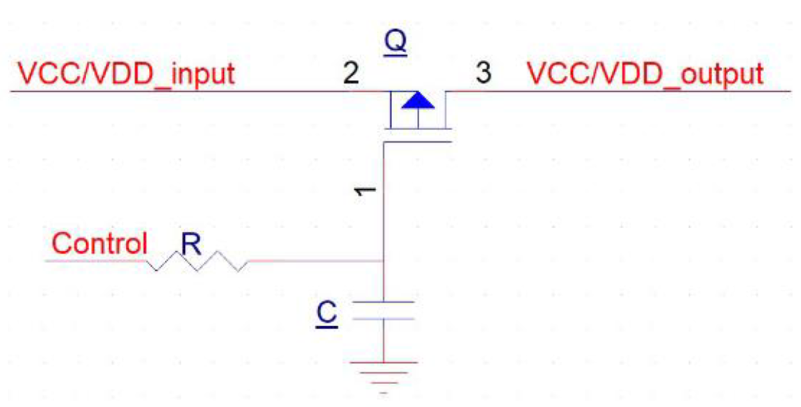
To handle inrush current, it is recommended to add a soft-start circuit when VCC/VDD os turned on, as seen below.
COG Initial
Notes
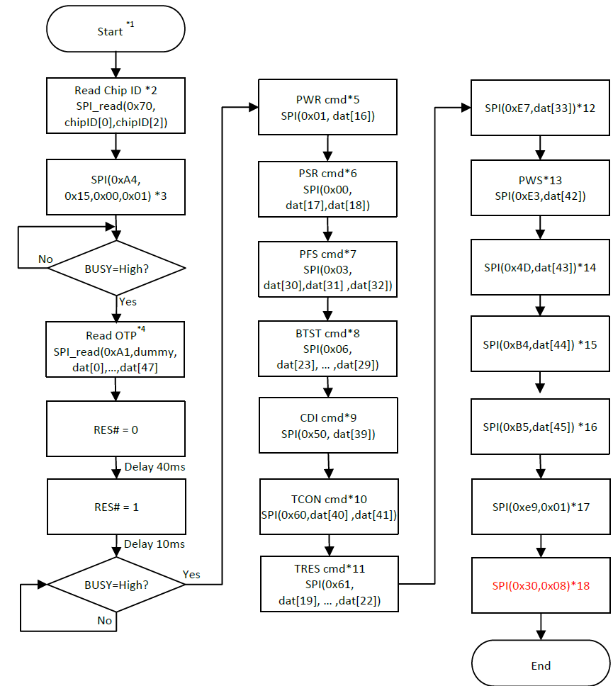
- Start: Follow the end of the power on sequence
- Chip ID: Chip ID of E2806 would be {0x03,0x02}
- This command is referred to Eink’s sample code. It should be applied for assigning the beginning address of OTP reading.
- Read OTP: the first byte of read out is dummy byte. According to the OTP mapping table, the necessary data is from 0x1500 ~ 0x152F, so there are 48 bytes data that need to be read out and store these data into the “dat” array.
- PWR: this is 1-byte data read from 0x1510 of OTP memory, which is equivalent to dat[16]
- PSR: this is 2-byte data read from 0x15110x1512 of OTP memory, which is equivalent to dat[1718]
- PFS: this is 2-byte data read from 0x151E0x1520 of OTP memory, which is equivalent to dat[3032]
- BTST: this is 7-byte data read from 0x15170x151D of OTP memory, which is equivalent to dat[2329]
- CDI: this is 1-byte data read from 0x1527 of OTP memory, which is equivalent to dat[39]
- TCON: this is 2-byte data read from 0x15280x1529 of OTP memory, which is equivalent to dat[4041]
- TRES: this is 4-byte data read from 0x15130x1516 of OTP memory, which is equivalent to dat[1922]
- The 0xE7 setting is 1-byte data read from 0x1521 of OTP memory, which is equivalent to dat[33]
- PWS: this is 1-byte data read from 0x152A of OTP memory, which is equivalent to dat[42]
- The 0x4D setting is 1-byte data read from 0x152B of OTP memory, which is equivalent to dat[43]
- The 0xB4 setting is 1-byte data read from 0x152C of OTP memory, which is equivalent to dat[44]
- The 0xB5 setting is 1-byte data read from 0x152D of OTP memory, which is equivalent to dat[45]
- The 0xE9 setting is 1-byte constant data of 0x01.
- The 0x30 setting is 1-byte constant data of 0x08.
Image Upload Process
This section describes how to send the image data into the COG driver which will update the display. The register index of image buffer is 0x10.
There is 2-bit data per pixel to define 4 colors. (e.g. the first byte represents the 1st ~ 4th pixels of the first line, the second byte represents the 5th ~ 8th pixels of the first line, …… and so on).
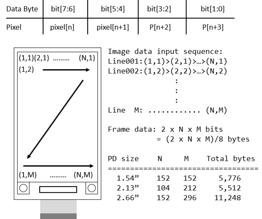
The color definition of image data is as shown below
| Data | Color |
|---|---|
| 00 | Black |
| 01 | White |
| 10 | Yellow |
| 11 | Red |
COG Update
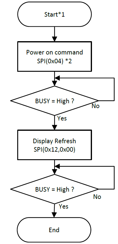
Warning
SPI(0x04) does not need data. Just the index.
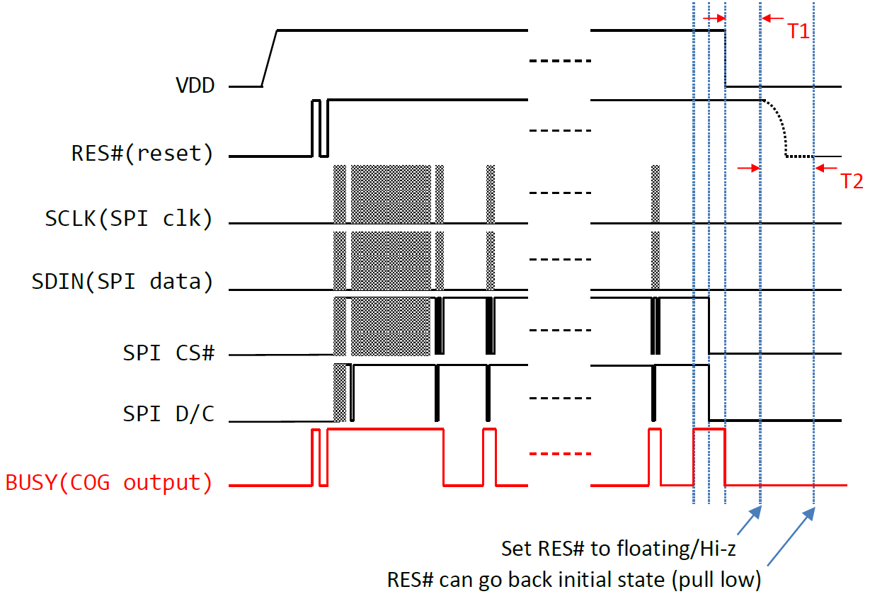
Turn off DC/DC
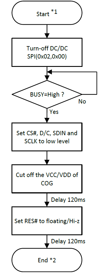
This power-off sequence is exactly based on the E5 SE 2.66” application note provided by E-ink. The real timing diagram is shown below. T1 and T2 must be more than 100ms at least.