SPI Timing Format
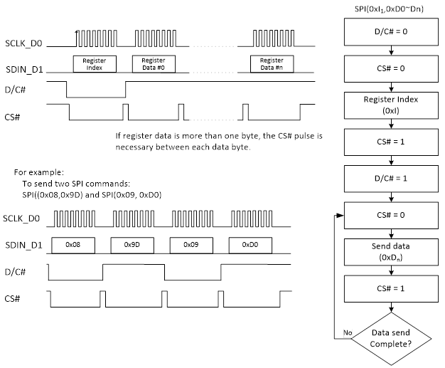
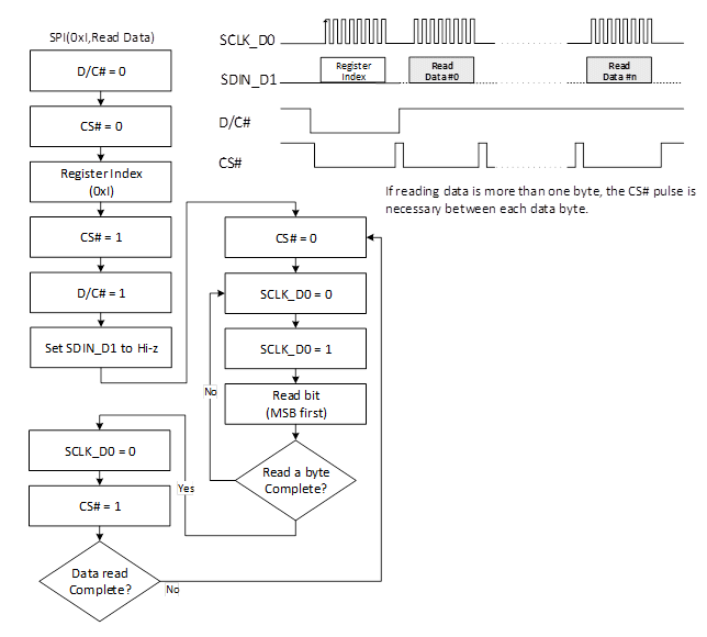
SPI commands are used to communicate between the host and the COG driver. The SPI format used differs from the standard in that two-way communications are not used.
When setting up the SPI timing, PDI recommends verifying both the SPI command format and the SPI command timing in this section.
| Step | Pin/Register | Data/Value | Name/Unit | Comment |
|---|---|---|---|---|
| SPI | 0x50 | 0x27 | Fast Update only | |
| SPI | 0x10 | Image array | DTM1 | Old image for Fast |
| SPI | 0x13 | Image array | DTM2 | New image for Fast |
| SPI | 0x50 | 0x07 | Fast Update only |
With
- Register is the register index, in the examples 0x50, 0x10, and 0x13.
- Data/Value could be
- A fixed value, in the example 0x27,
- Multiple values, in the example DTM1 and DTM2 for image data array,
- The D/C line is pulled LOW for command and HIGH for data.
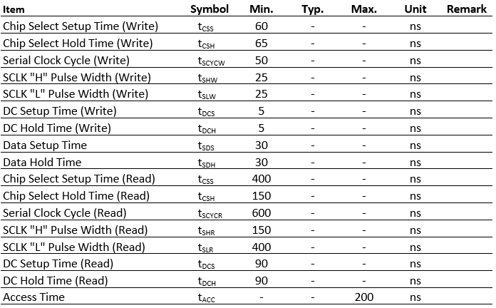
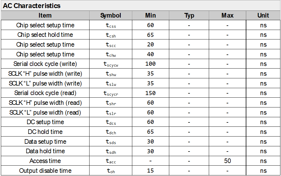
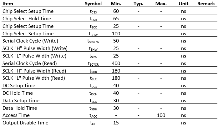
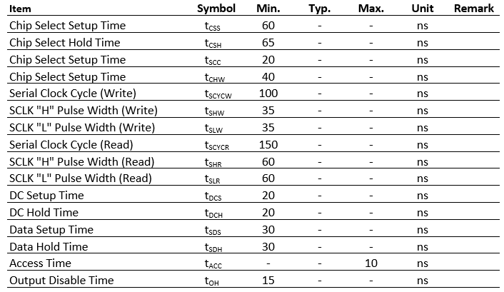
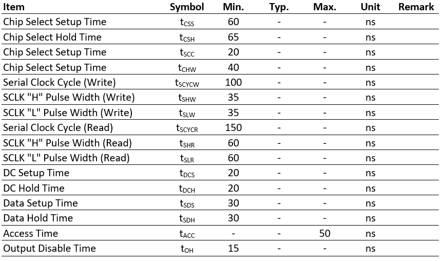
SPI Command Timing
The following specifications apply for VDDIO - GND = 2.3V to 3.6V, TOPR = 25°C, CL=20pF


AC Characteristics
1.54”, 2.13”
1.52”, 2.06”
2.66Ӧ
2.9Ӧ
4.2Ӧ
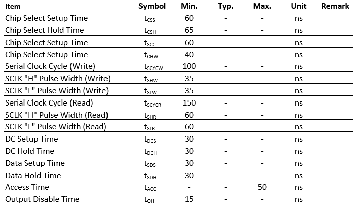
4.37Ӧ