SPI Timing Format
SPI commands are used to communicate between the host and the COG driver. The SPI format used differs from the standard in that two-way communications are not used.
When setting up the SPI timing, PDI recommends verifying both the SPI command format and the SPI command timing in this section.
SPI pin definition
- SCLK - serial peripheral interface clock
- SDIN - serial peripheral interface data
- D/C# - serial peripheral interface command and data pin
- M_CS# - master panel chip select
- S_CS# - slave panel chip select
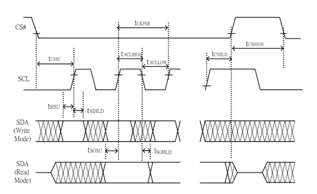
The maximum clock speed of the display is 20MHz (Write), 2.5MHz (Read).
| Step | Register | CS pin | Data/Value | Name/Unit | Comment |
|---|---|---|---|---|---|
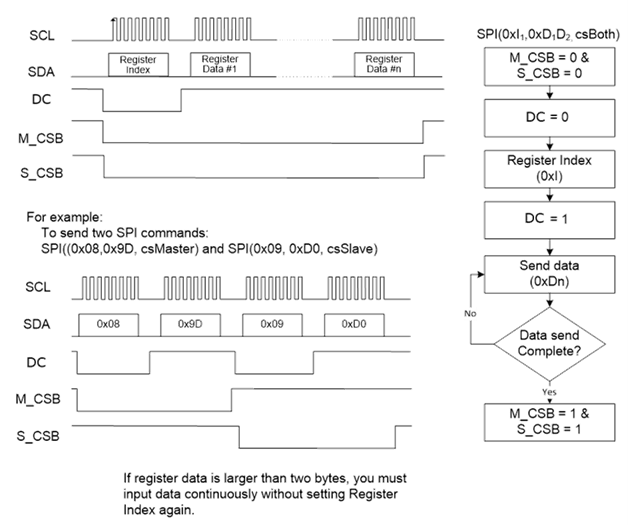
| SPI | 0x01 | Both | OTP[0x10], 0x00 | DCTL | 2 bytes of data, first DCTL then 0x00 |
- Register is the register index, in the example above 0x01
- CS Pin indicates which driver is selected for command:
- Master : only deliver to Master driver
- Slave : only deliver to Slave driver
- Both : deliver to both Master and Slave
- Selecting the proper driver requires toggling both Master and Slave CS pins, as seen in the flowchart below
- Data/Value could be
- A fixed value, for example 0x00
- Values read from the OTP memory at OTP index
- Multiple values, in the example the OTP value from address 0x10 and 0x00
- The D/C line is pulled LOW for command and HIGH for data.
SPI Command Timing
The following specifications apply for VDDIO - GND = 2.3V to 3.6V, TOPR = 25°C, CL=20pF