EPD Update Procedure
The update procedure includes 8 steps as shown on the right side.
- Power on screen
- Reset the CoG driver
- Read the OTP data
- Initialize the COG driver
- Send the image
- Update the COG
- Stop DC/DC
- Power off screen
Power on screen
The initial state before start has VCC/VDD, /RESET, D/C, /CS, SDA, SCL kept at 0V.
In order to the inrush current will cause other issue. It is recommended to add start DC/DC when VCC/VDD is turned on.
Perform in the following order.
| Step | Pin/Register | Data/Value | Name/Unit | Comment |
|---|---|---|---|---|
| GPIO | POWER | HIGH | External MOSFET power driver | |
| GPIO | D/C | HIGH | Data if HIGH, command if LOW | |
| GPIO | /RESET | HIGH | Panel reset, active LOW | |
| GPIO | Panel /CS | HIGH | SPI chip select, active LOW | |
| GPIO | !BUSY | INPUT | Input, floating | |
| SPI | CLK | SPI clock | ||
| SPI | SDA | SPI data |
Reset the CoG driver
Note
Included in function COG_reset()
| Step | Pin/Register | Data/Value | Name/Unit | Comment |
|---|---|---|---|---|
| GPIO | POWER | HIGH | Set POWER HIGH | |
| Delay | 200 | ms | Make sure POWER is stable | |
| GPIO | RESET | HIGH | Set RESET HIGH | |
| Delay | 2 | ms | ||
| GPIO | RESET | LOW | Set RESET LOW | |
| Delay | 4 | ms | ||
| GPIO | RESET | HIGH | Set RESET HIGH | |
| Delay | 20 | ms |
Proceed to next step “Read the OTP data”.
If the OTP data is already read and available, proceed to Initialise the COG driver.
Read the OTP data
Note
Included in function COG_getDataOTP()
This step is performed once, as long as the host retains the values. If the host loses the values, the host should perform this step again.
Info
The maximum clock speed of the display is 2.5MHz (Read).
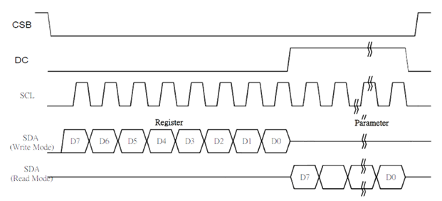

Read operation of 4-line SPI
| Step | Pin/Register | Data/Value | Name/Unit | Comment |
|---|---|---|---|---|
| GPIO | /CS | LOW | Select | |
| GPIO | D/C | LOW | Command mode | |
| SPI3 | 0xb9 | SPI3 = SCK, SDIO, CS plus D/C | ||
| GPIO | D/C | HIGH | Data mode | |
| SPI3 | Read 1 byte | Read dummy data | ||
| SPI3 | Read 128 bytes | Read 128 bytes of data | ||
| GPIO | /CS | HIGH | Unselect |
Store the OTP data in memory to avoid reading it at each update.
Check Chip ID or the COG type byte to confirm the OTP data is appropriate to your chosen size:
| Size n | 3.4” | 5.8” or 7.4" |
|---|---|---|
| Chip ID (0x00) | 0x17 | 0x16 |
| COG Type (0x01) | 0x97 | 0x95 |
Proceed to next step Initialise the COG driver.
Initialize the COG driver
Note
Included in function COG_initial()
Warning
The maximum clock speed of the display is 20MHz (Write).
| Step | Register | CS pin | Data/Value | Name/Unit | Comment |
|---|---|---|---|---|---|
| SPI | 0x01 | Both | OTP[0x10], 0x00 | DCTL | 2 bytes of data, first DCTL then 0x00 |
Send the image
Note
Included in function COG_sendImageDataNormal() and function COG_sendImageDataFast()
| Step | Pin/Register | Data/Value | Name/Unit | Comment |
|---|---|---|---|---|
| SPI | 0x13 | OTP[0x15+6] | DUW+6 | DUW: there is 6 bytes’ data that are read from 0x15…0x1A of OTP memory. |
| SPI | 0x90 | OTP[0x0c+4] | DRFW+4 | DRFW: there is 4 bytes’ data that are read from 0x0C…0x0F of OTP memory. |
| SPI | 0x12 | OTP[0x12+3] | DRFW+3 | RAM_RW: there is 3 bytes’ data that are read from 0x12…0x14 of OTP memory. |
| SPI | 0x10 | DRAM1+n | DRAM1: the data is the NEW image data that you want displaying next moment. | |
| SPI | 0x12 | OTP[0x12+3] | DRFW | RAM_RW: there is 3 bytes’ data that are read from 0x12…0x14 of OTP memory. |
| SPI | 0x11 | DRAM2+n | Normal update – See note below DRAM2 image is dummy data. It just needs to be filled with the enough amount of 0x00. |
|
| Fast update – See note below DRAM2 image is the OLD image data that already displayed on the EPD. |
Content of DRAM1 and DRAM2
| Normal update | Fast update | |
|---|---|---|
| DRAM1 | DRAM1: the data is the NEW image data that you want to display next moment. | DRAM1: the data is the NEW image data that you want displaying next moment. |
| DRAM2 | Normal update – DRAM2 image is dummy data. It just needs to be filled with the enough amount of 0x00. | Fast update – DRAM2 image is the OLD image data that already displayed on the EPD. |
Note
Image order is important when calling Fast Update, especially when used in succession. Unlike with Normal Update, two images are always used with Fast Update: the old and new images. Note that the new image of the first Fast Update call becomes the old image of the second succeeding Fast Update call.
Neglecting this order will result to ghosting and improper image display.
| Size n | 3.4” | 5.81” | 7.41” |
|---|---|---|---|
| DRAM1 | 22344 bytes | 23040 bytes | 48000 bytes |
| DRAM2 | 22344 bytes | 23040 bytes | 48000 bytes |
The EPD needs to receive both first and second frame data each updating.
The index of the first frame is 0x10 and the second frame is 0x11.
The data of image frame, one bit represents 1 pixel.
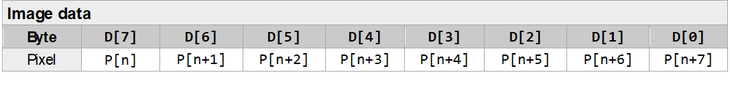
Example
The first byte represents the 1st…8th pixels of the first line.
The second byte represents the 9th…16th pixels of the first line, and so on.
Data 1 represents a black colour pixel and data 0 represents a white colour pixel.
Update the COG
Note
Included in function COG_update()
| Step | Pin/Register | Data/Value | Name/Unit | Comment |
|---|---|---|---|---|
| SPI | 0x05 | 0x7d | ||
| Delay | 50 | ms | ||
| SPI | 0x05 | 0x00 | ||
| Delay | 1 | ms | ||
| SPI | 0xd8 | OTP[0x1c] | MS_SYNC | MS_SYNC is read from 0x1C of OTP memory |
| SPI | 0xd6 | OTP[0x1d] | BVSS | BVSS is read from 0x1D of OTP memory |
| SPI | 0xa7 | 0x10 | ||
| Delay | 2 | ms | ||
| SPI | 0xa7 | 0x00 | ||
| Delay | 10 | ms | ||
| SPI | 0x44 | 0x00 | ||
| SPI | 0x45 | 0x80 | ||
| SPI | 0xa7 | 0x10 | ||
| Delay | 2 | ms | ||
| SPI | 0xa7 | 0x00 | ||
| Delay | 10 | ms | ||
| SPI | 0x44 | 0x06 | ||
| SPI | 0x45 | indexT | Normal update – See note below indexT = 0x28 + tempC |
|
| Fast update – See note below indexT = tempC + 0x28 +0x80 |
||||
| SPI | 0xa7 | 0x10 | ||
| Delay | 2 | ms | ||
| SPI | 0xa7 | 0x00 | ||
| Delay | 10 | ms | ||
| SPI | 0x60 | OTP[0x0b] | TCON | TCON is read from 0x0B of OTP memory |
| SPI | 0x61 | OTP[0x1b] | STV_DIR | STV_DIR is read from 0x1B of OTP memory |
| SPI | 0x02 | OTP[0x11] | VCOM | VCOM is read from 0x11 of OTP memory |
| SPI | 0x03 | OTP[0x1f] | VCOM_CTRL | VCOM_CTRL is read from 0X1f of OTP memory |
Calculation of TSSET from tempC temperature in C
Note
TSSET refers to the ambient temperature. This value comes from your chosen external temperature sensor. Default value in our demo is 25C. Update this when working outside room temperature range.
| Normal update | Fast update | |
|---|---|---|
| Definition | TSSET is an index of the normal update. | TSSET is an index of the fast update. |
| Range | The acceptable range of temperature is -15°C to +60°C and 1°C per step. | The acceptable range of temperature is +0°C to +50°C and 1°C per step. |
| Check tempC | -15 <= tempC <= +60 | 0 <= tempC <= +50 |
| Value TSSET | TSSET = 0x28 + tempC | TSSET = (tempC + 0x28) + 0x80 |
| Low value check | if TSSET < 0x25, TSSET = 0x25 | if TSSET < 0xa8, TSSET = 0xa8 |
| High value check | if TSSET > 0x64, TSSET = 0x64 | if TSSET > 0xda, TSSET = 0xda |
Danger
Operating outside the acceptable temperature range may damage the panel.
Start DC/DC
There are 32-bytes data for describing the sequence of soft-start.
| Entry | Data/Value | Comment |
|---|---|---|
| Stage 1 | OTP[0x28+8] | Stage 1 of DC/DC sequence |
| Stage 2 | OTP[0x30+8] | Stage 2 of DC/DC sequence |
| Stage 3 | OTP[0x38+8] | Stage 3 of DC/DC sequence |
| Stage 4 | OTP[0x40+8] | Stage 4 of DC/DC sequence |
The full sequence has 4 stages.
The parameters for each stage take 8 bytes. There are two formats for the stage.
The REPEAT field contains the data format used for this stage and the number of times to repeat it.
- Bit 7 MSB defines the format used in this stage. It should be 1.
- Bits 6 to 0 contain the number of times to repeat.
| Bit | 7 | 6 | 5 | 4 | 3 | 2 | 1 | 0 |
|---|---|---|---|---|---|---|---|---|
| REPEAT | FORMAT | Number of times to repeat the sequence | ||||||
| 1 | nREPEAT = REPEAT & 0x7f | |||||||
Example
0x87 or 0b10000111 means repeat the sequence 7 times.
Danger
If bit 7 MSB of REPEAT is equal to 0, please contact support.
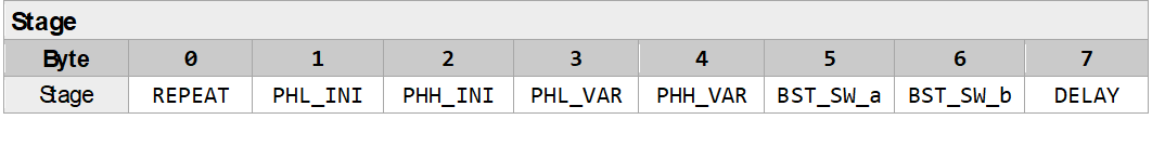
The content of the stage includes 8 bytes.
Format1
| Byte | Field | Comment | Used by register |
|---|---|---|---|
| 0 | FORMAT = REPEAT & 0x80 | Must be 0x80 | |
| nREPEAT = REPEAT & 0x7f | Define the number of times to repeat the stage | ||
| 1 | PHL_INI | Define the initial value of PHL, the first data of the register 0x51 | 0x51 |
| 2 | PHH_INI | Define the initial value of PHH, the second data of the register 0x51 | 0x51 |
| 3 | PHL_VAR | The byte represents the changing value of PHL with each iteration REPEAT iteration | |
| 4 | PHH_VAR | The byte represents the changing value of PHH with each REPEAT iteration | |
| 5 | BST_SW_a | Set the power on/off manager at the start of the phase | 0x09 |
| 6 | BST_SW_b | Set the power on/off manager at the end of the phase | 0x09 |
| 7 | SCALE = DELAY & 0x80 | The scale for delay time at the end of the stage | |
| nDELAY = DELAY & 0x7f | The delay time at the end of the stage |
Both PHL_VAR_n and PHH_VAR_n could be negative numbers, represented by a 2’s complement.
Example
-5 equals 0xfb
The DELAY field contains the scale and the duration of the delay for the end of the stage.
- Bit 7 defines the scale of the delay. It should be 1.
- Bits 6…0 contain the duration of the delay.
The DELAY field includes the scale in bit 7 and the delay time in bits 6…0 for the end of the stage.
| Bit | 7 | 6 | 5 | 4 | 3 | 2 | 1 | 0 |
|---|---|---|---|---|---|---|---|---|
| DELAY | SCALE | DELAY & 0x7f Delay time | ||||||
| 1 | Scale in milliseconds, nDELAY = DELAY & 0x7f ms | |||||||
Example
0x82 or 0b10000010 means a delay of 2 ms.
Danger
If bit 7 MSB of DELAY is equal to 0, please contact support.
For each of the four stages,
- Set the variables
| Step | Variable | Data/Value | Name/Unit | Comment |
|---|---|---|---|---|
| Calculate | FORMAT | STAGE[0x00] | FORMAT = STAGE[0x00] & 0x80 = 0x80 | |
| Calculate | nREPEAT | STAGE[0x00] | nREPEAT = STAGE[0x00] & 0x0f | |
| Calculate | iPHL | STAGE[0x01] | iPHL = STAGE[0x01] = PHL_INI | |
| Calculate | iPHH | STAGE[0x02] | iPHH = STAGE[0x02] = PHH_INI | |
| Calculate | PHL_VAR | STAGE[0x03] | PHL_VAL = STAGE[0x03] | |
| Calculate | PHH_VAR | STAGE[0x04] | PHH_VAR = STAGE[0x04] | |
| Calculate | BST_SW_a | STAGE[0x05] | BST_SW_a = STAGE[0x05] | |
| Calculate | BST_SW_b | STAGE[0x06] | BST_SW_b = STAGE[0x05] | |
| Calculate | SCALE | STAGE[0x07] | SCALE = STAGE[0x07] & 0x80 | |
| Calculate | nDELAY | STAGE[0x07] | ms | nDELAY = STAGE[0x07] & 0x7f |
- Repeat the loop
nREPEATtimes
| Step | Pin/Register | Data/Value | Name/Unit | Comment |
|---|---|---|---|---|
| SPI | 0x09 | BST_SW_a | ||
| Calculate | iPHL | Variable iPHL = iPHL + PHL_VAL | ||
| Calculate | iPHH | Variable iPHH = iPHH + PHH_VAL | ||
| SPI | 0x51 | iPHL | ||
| iPHH | ||||
| SPI | 0x09 | BST_SW_b | ||
| Delay | nDELAY | ms | if SCALE = 0x80 |
Send the update command
| Step | Register | CS Pin | Data/Value | Name/Unit | Comment |
|---|---|---|---|---|---|
| GPIO | !BUSY | HIGH? | Wait for !BUSY = HIGH | ||
| SPI | 0x15 | Both | 0x3c |
Stop DC/DC
Note
Included in function COG_stopDCDC()
| Step | Pin/Register | Data/Value | Name/Unit | Comment |
|---|---|---|---|---|
| GPIO | !BUSY | HIGH? | Wait for !BUSY = HIGH | |
| SPI | 0x09 | 0x7f if 5.8"/7.4" 0x7b if 3.4" |
||
| SPI | 0x05 | 0x3d | ||
| SPI | 0x09 | 0x7e if 5.8"/7.4" 0x7a if 3.4" |
||
| Delay | 60 | ms | ||
| SPI | 0x09 | 0x00 |
Power off screen
Set all the GPIO pins to LOW.
| Step | Pin/Register | Name/Unit | Name/Unit | Comment |
|---|---|---|---|---|
| GPIO | D/C | LOW | Data if HIGH, command if LOW | |
| GPIO | /RESET | LOW | Panel reset, active low | |
| GPIO | Panel /CS | LOW | SPI chip select, active low | |
| GPIO | !BUSY | Input, floating | ||
| GPIO | POWER | LOW | External MOSFET power driver | |
| SPI | CLK | SPI clock | ||
| SPI | SDA | SPI data |
The EPD update procedure is completed.