SPI Timing Format
SPI commands are used to communicate between the host and the COG driver. The SPI format used differs from the standard in that two-way communications are not used.
When setting up the SPI timing, PDI recommends verifying both the SPI command format and the SPI command timing in this section.
SPI pin definition
- SCLK - serial peripheral interface clock
- SDIN - serial peripheral interface data
- D/C# - serial peripheral interface command and data pin
- CS# - panel chip select
The maximum clock speed of the display is 20MHz (Write), 2.5MHz (Read).
| Step | Pin/Register | Data/Value | Name/Unit | Comment |
|---|---|---|---|---|
| SPI | 0x50 | 0x27 | Fast Update only | |
| SPI | 0x10 | Image array | DTM1 | Old image for Fast |
| SPI | 0x13 | Image array | DTM2 | New image for Fast |
| SPI | 0x50 | 0x07 | Fast Update only |
with
-
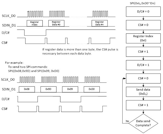
Register is the register index, in the examples
0x50,0x10, and0x13. -
Data/Value could be
-
A fixed value, in the example
0x27, -
Multiple values, in the example
DTM1andDTM2for image data array,
-
-
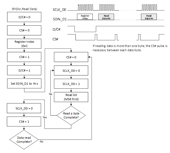
The D/C line is pulled
LOWfor command andHIGHfor data.
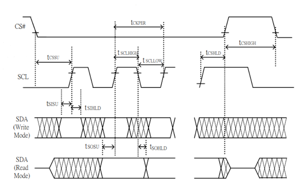
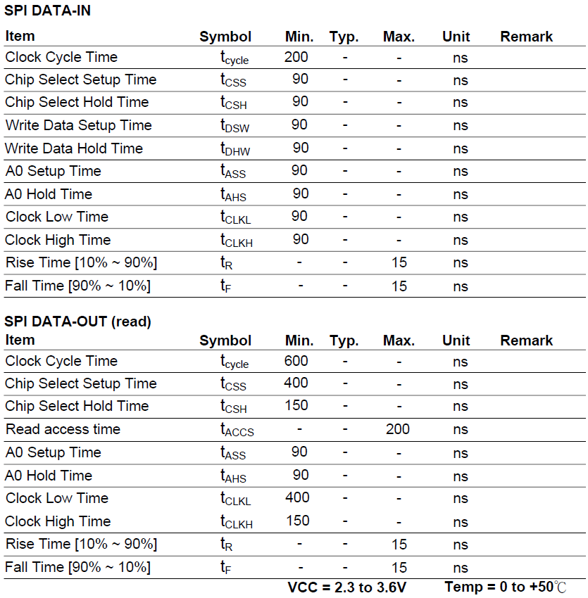
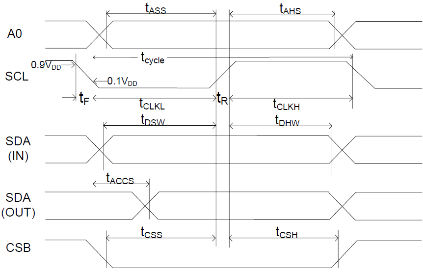
SPI command timing
The following specifications apply for VDDIO - GND = 2.3V to 3.6V, TOPR = 25°C, CL=20pF
3.4Ӧ
5.8”, 7.4”